Eagle CAD
- tags Electronics design Circuit Design
- Resources
- Notes
- PCB layout
- Sparkfun PCB layout
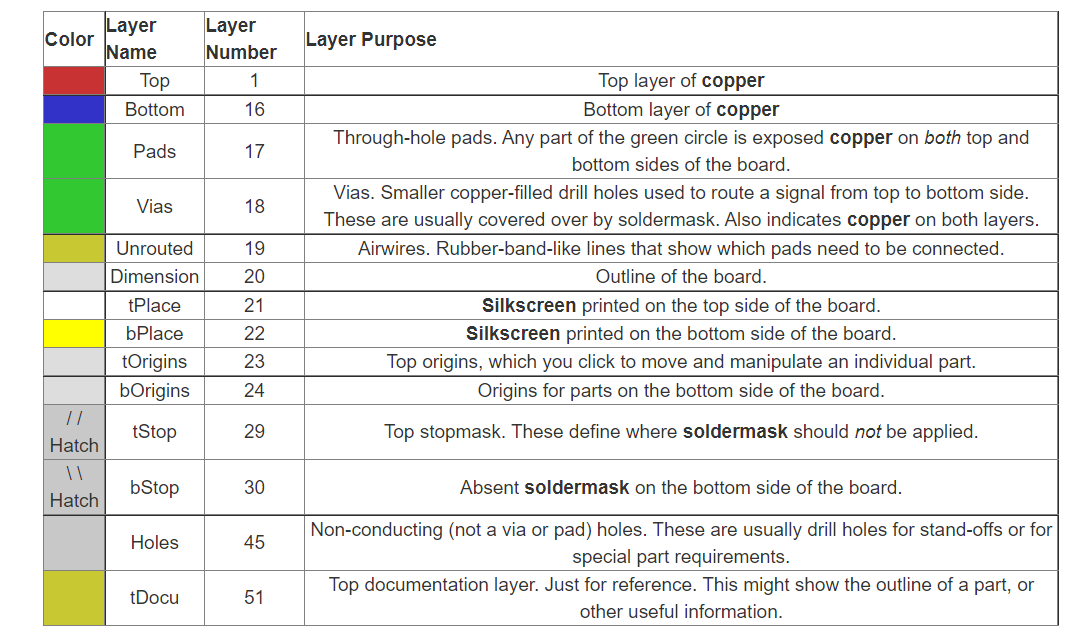
- layer Tdocu shows where the actual components sit on the foot print, change to a bright colour to see them.
- Define net classes to give separate routing conditions for each class of components like the power and signal traces.
- A trace with many right angles in them will tend to round the edges of a square wave signal and will cause the microcontroller to not read them properly. This is a probabilistic issue, may not happen.
- Its not good practice to put capacitors in an array far away from the microcontroller, you want to keep the traces short.
- when feeding power, you want to keep the input power supply stack to one side and feed all the components in a star configuration.
- Watch for ground return paths, its the path the current takes to get back to the regulator/supply, if you have a lot of traces in the bottom, some can create pinch points in the ground plane. Need to take care for high current paths.
- Try to lay all the signal traces first on the top layer, and gnd layer on botton. if four layer board, then signal, gnd, vcc, bottom layer.
- Workflow
- New Project > New schematic
- Add components from Libraries, move rotate, copy them.
- Use net tool to link components
- Smash tool to edit the positions of the labels
- put values in the label to define them.
- Use Alt to move in finer spacing.
- F7 to use the move command
- F4 to go to name mode
- F5 to go to value mode
- F8 rats nest
- F9 route
- Alt+F9 ripup
- Click an air wire and click ‘i’ to get the properties, you can disable air wire if needed.
- When routing hold the shift key and click to drop a via, use the middle mouse button to drop to the bottom of the layer
- Selecting overlapping layers in board view, left click to select, right click to alternate between parts.
- Routing, to get a via, start a trace and change layer manually or use the middle mouse button.
- After routing, click ratsnest and check bottom status, it should say noting to do.
- To make a ground pour, draw a polygon next to the dimension line, use the isolate settings at the top to adjust the clearance, and use the name tool to name it as GND, last-click ratsnest to fill the ground pour. Good practice to have ground pours on both sides of the board.
- PCB layout
-
tags design Electronics Mechatronics Mechatronica M10V pick and place Eagle CAD
- Eagle CAD
Notes mentioning this note
Archive
When a Note reaches a significant size they are indexed into the Archive. This is the only place where a...
Circuit Design
tags design Electronics Mechatronics Mechatronica M10V pick and place Eagle CAD Resources Beginning Embedded Electronics Sparkfun Ultralibrarian parts eagle library...
Eagle CAD
tags Electronics design Circuit Design Resources Autodesk Eagle Tutorials Fab academy Introduction to Eagle CBA Fab Eagle library Fab Eagle...
Electronics
tags: Circuit Design Resources All about Circuits: Electronics Basics Electronics for Geeks Physics Videos by Eugene #Youtube courses watch Electronics...
Mechatronica M10V pick and place
Resources M10V setup Happy Onam with Mechatronika a short video we did for Onam celebrations with the Mechtronika. Notes SMD...
Mechatronics
tags Robotics
J Edward Carryer Stanford
Introduction to Mechatronics J Edward carryer
Pippet Jockey Medical robots